A TSMC 2nm manufacturing guide matters because the next chip cycle will not be won by a single benchmark score. It will be shaped by whether designers can turn a new transistor architecture into reliable, affordable volume production. That affects the phones, laptops, AI servers, cars, and edge devices that arrive over the next several years.
TSMC’s N2 process is the company’s first major move to gate-all-around transistor technology, also called nanosheet transistors. The label “2nm” is marketing shorthand, not a literal measurement of a transistor feature. Still, the transition is consequential. It changes how leading chips control electrical current, how designers manage power, and how manufacturers protect yields while complexity climbs.
What Changes in TSMC 2nm Manufacturing
For several generations, advanced logic chips relied on FinFET transistors. A FinFET uses a vertical fin as the channel through which current flows, with the gate controlling current from multiple sides. That approach delivered extraordinary scaling, but the geometry becomes harder to control as devices shrink.
N2 replaces that structure with horizontal nanosheets. The gate wraps around each sheet, giving it tighter control over current flow. Better control lets chip designers reduce leakage, improve performance at a given power level, or lower power at a similar performance target. Those are the three levers that matter in modern silicon economics.
TSMC has publicly positioned N2 as a full-node transition, not a minor refinement of its 3nm family. Its early N2 manufacturing approach retains frontside power delivery, meaning data signals and power connections are routed through the conventional side of the wafer. That choice is strategic. It reduces transition risk for customers moving from established design flows while still delivering the benefits of nanosheet transistors.
The next step is N2P, a performance-enhanced version of N2, followed by the A16-class process with backside power delivery, which TSMC calls Super Power Rail. Backside power moves power wiring to the reverse side of the silicon, relieving congestion on the front side where signal routing competes for space. It is a major architectural change, particularly useful for dense, high-performance compute blocks.
Why the Nanosheet Shift Is Harder Than a Shrink
Leading-edge chipmaking is a tightly coupled system. A better transistor does not automatically produce a better product if the wiring, SRAM cells, power network, design tools, and packaging cannot keep pace.
The first problem is process integration. Nanosheets require layers to be grown, patterned, etched, released, and wrapped with gate material at extreme precision. Small variation across a wafer can affect transistor behavior. At mature nodes, manufacturers have decades of accumulated margin. At 2nm-class nodes, each process window is narrower and defects are more expensive.
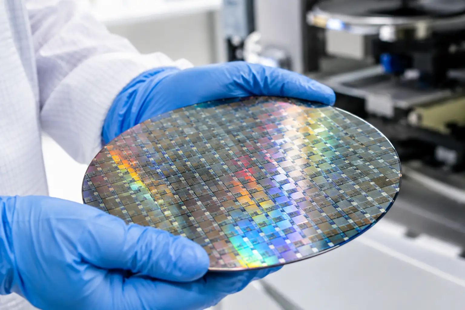
The second problem is yield. A wafer can contain hundreds of advanced processors, but only functional die can be sold. Yield is not a footnote in this business. It determines whether a premium smartphone chip is financially viable and whether an AI accelerator can be supplied at the scale cloud operators demand. TSMC’s value is not merely its ability to demonstrate a node. It is its ability to make that node predictable at high volume.
The third problem is design enablement. Customers need validated process design kits, standard cell libraries, SRAM macros, IP blocks, and electronic design automation support long before their chip reaches a fab. This creates a timing gap that consumers rarely see. A node may enter production, yet the most ambitious designs can take another cycle to appear because teams need time to close timing, power, area, and verification targets.
The Real Product Is a Manufacturing Platform
Consumers tend to compare chips by nanometer labels. Product teams should think in platforms. At N2, transistor density is only one input. The finished result depends on design rules, wafer capacity, advanced packaging availability, test capacity, and the customer’s ability to design a chip that can actually be cooled and powered.
For a smartphone processor, the practical goal may be longer sustained performance within a fixed thermal envelope. For a laptop chip, it may be lower idle power and more battery life. For an AI accelerator, the limiting factor might not be raw compute density at all. It may be memory bandwidth, interconnect, power delivery, or the availability of high-bandwidth memory and advanced packaging.
This is why TSMC’s 2nm transition should be read alongside its packaging roadmap. Chiplets allow companies to place different functions on separate pieces of silicon, then connect them in a package. A leading-edge compute tile can sit beside I/O die made on a less expensive node. That reduces cost, improves yield, and lets teams reserve 2nm capacity for the logic that benefits most from it.
The trade-off is complexity. Packaging is no longer an afterthought attached to the end of fabrication. It becomes part of electrical design, thermal design, supply planning, and product timing. A company can have a finished 2nm compute die and still miss a launch window if packaging or memory supply is constrained.
How to Read the TSMC 2nm Roadmap
The useful question is not whether 2nm is “real.” The useful question is which version of the platform a chipmaker is using and what problem it is trying to solve.
TSMC began N2 volume production on its publicly stated schedule in the second half of 2025. During 2026, the market should expect the node’s impact to become more visible through design ramps, capacity expansion, and product announcements. N2P is positioned as the next refinement, while the A16 generation introduces a more aggressive power-delivery architecture aimed at demanding compute designs.
That sequence matters. N2 is likely to serve customers that want the benefits of gate-all-around technology without taking on the additional integration burden of backside power. A16 is more compelling where power routing is a primary bottleneck and the product’s economics can absorb a more complex manufacturing path.
Do not assume every flagship device will move immediately. Leading nodes carry higher wafer costs, and not every chip gains enough from the transition. Connectivity controllers, analog components, power management, display drivers, and many I/O functions often make better financial sense on older processes. The winning design strategy is selective, not ideological.
Four Signals Worth Watching
If you are following the semiconductor market, four indicators tell a clearer story than node labels alone:
- Yield and capacity commentary. A rapid ramp with stable yields indicates that the manufacturing process is moving beyond early adopter status.
- Customer adoption. High-volume mobile and compute customers validate the design ecosystem and create demand for additional capacity.
- Advanced packaging availability. AI products depend on packaging and memory as much as transistor scaling.
- Power efficiency in real devices. Battery life, sustained performance, and data-center watts per unit of work reveal more than brief benchmark spikes.
These signals also explain why a seemingly modest process improvement can have outsized commercial consequences. If a chip can deliver the same user experience while using less energy, it can reduce cooling requirements, extend battery life, increase server density, or create room for more on-device AI work. Those gains compound across a product line.
What 2nm Means for Buyers and Builders
For consumers, 2nm should eventually translate into devices that do more within the same heat and battery limits. The first products may emphasize performance, but the more durable benefit is efficiency. That is especially relevant as local AI features place sustained demands on phones and PCs.
For founders, operators, and technology teams, the lesson is broader. Hardware roadmaps now affect software decisions earlier. AI workloads that were impractical on a laptop or handheld device may become commercially reasonable as efficiency improves. But teams should not build plans around a node name alone. Profile the workload, identify memory and power constraints, and keep a cloud fallback where latency, privacy, or device cost does not justify local processing.
TSMC’s 2nm era is not just another annual spec bump. It is a test of whether transistor innovation, power architecture, design tools, and packaging can move in formation. The companies that benefit most will be the ones that treat advanced silicon as a system decision, then build products that make every milliwatt count.